
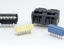
Connector Pitch is the measurement from the center of one contact to the center of the next contact. When a connector has multiple rows, the pitch in each row and the pitch between rows may be different. 1. Space Constraints – The smaller the pitch, the smaller the connector can be. As well as, smaller pitch can provide a higher variety of contacts inside the identical area. 2. Electrical Parameter – Pitch dimension has a optimistic correlation to electrical specs reminiscent of present score and dielectric withstanding. 3. Other Physical Constraints – Depending on the design, Greenconn offers numerous low-profile connector choices throughout all pitches. We also settle for customization requests. Greenconn presents headers and recepticles in single, double, triple, and quadruple row configurations. Single and dual rows are fashionable choices, whereas triple and quadruple rows are supplied in a smaller variety of pitch and style options. What are the Connector SMT PCB connector Contact Materials and Plating?
Our connectors typically use a copper alloy as the bottom material for his or her contacts (pins). However, totally different alloy supplies provide various levels of conductivity efficiency and bodily endurance. Plating impacts the connector’s efficiency, life cycle, quality, and value. Underplating is used to boost the efficiency. This course of varieties an internal diffusion barrier (Zn and Cu by gold) and prevents pollutants from reacting with base metals. It additionally acts as a medium to help the end plating adhere to the base material. Finish plating is the second step of the plating process that helps strengthen the electrical conductivity. There are numerous choices for end plating, depending on the design necessities and finances. Tin will be further characterized as brilliant tin or matte tin. Bright tin might be simply identified by its glossy texture. It really works well against corrosion, whereas sacrificing its solderability. Matte tin, versus shiny tin, has a dull texture, which isn’t as appealing as the bright tin. However, it affords a great level of protection against corrosion without sacrificing its solderability. Any such plating gives tin plating on the tail and gold plating on the contact area. It offers an excellent steadiness between the advantages of gold and the lower price of tin. Greenconn also presents more than simply the usual gold and tin plating choices. For more information on plating, please contact us as http://www.Greenconn.comen/contact.htm . Insulators are basic to board-to-board connectors. They are used to hold the conductors, or pins, collectively to create the desired shape of the connectors. Different insulators also perform in another way relating to to their energy, weatherability, and chemical resistance.
Layout of the three PCBs has progressed very quickly – far quicker than the time taken to develop the casework, by literally an order of magnitude. The boards are being done as 2-layer PCBs. It’s wonderful to find that the cost of 5 prototype 2-layer PCBs is around $50 for a 48-hour turnaround. In comparison with $500 for even a 4-layer PCB that takes over a month to be delivered, the choice to try to make all of the PCBs as 2-layer makes a number of sense. The Laptop’s PCBs are divided into three elements, for a number of causes. Firstly: to put all of the elements onto a single 12in-lengthy PCB doesn’t make sense. The form can be flimsy, awkward to chop, and would have significant void areas. Secondly: the facility PCB for the Battery Charger IC must be 2oz copper (it’s coping with 15 watts) whereas the rest of the design does not.
Thirdly: there are structural dividers and supports in the best way, and fourthly: the PCB with the STM32F072 (for a keyboard controller, touchpanel, Real-time Clock and Power Manager) has to be at a special top from the opposite PCBs. The truth that this enables for a lower value of improvement, lower threat, in addition to design re-use is nearly incidental. PCB1 accommodates the EOMA68 CPU Card slot, in addition to all the main user-going through I/O: USB ports, USB Audio, LVDS IC for the LCD, Headphone, Mic, speakers, Micro-SD card slot. The USB connectors can be seen in the highest left corner: two dealing with inwards into the interior compartment, and one dealing with outwards. Micro-SD and Headphone/Mic jack may be seen in the highest left. The IC in the center, below the Headphone jack, is the CM108AH audio IC, and the elements in between are mostly the 2 0. If you have any kind of concerns pertaining to where and ways to use PCB connector assembly (click the next post), High-speed PCB connector you could call us at the web site. 5 watt TDA2822 amplifiers, for the audio system.